

Entries tagged FPGA
Hacks of 2015
28 December 2015 (programming haskell idris games electronics avr FPGA meta)Encsé writes in his blog that one of the reasons he created a tiny CPS-based Scheme interpreter was because he realized he hasn't done any fun side projects all year. So I thought I'd make an inventory of fun hacks I've done in 2015.
Bit-fiddling
- An FPGA implementation of the Commodore PET. This is still not fully finished: although I managed to hunt down the bug mentioned at the end of the blog post, I still haven't gotten around to implementing Datasette (tape) I/O.
-
Viki & I put together a prototype for an AVR-based CHIP-8
handheld. This one has no web presence yet; we're hoping to
finalize the design into a PCB-based one, before releasing the
schematics and the code.

- Went to a hackerspace.sg workshop/hackathon for the Fernvale platform. Not much came out of that, I think I was the only person who at least got as far as running my own code on the device (reusing the low-level bitbanging from Fernly of course). I ended up doing some lame but colourful animations on the screen that would have gotten me boo'd off the stage in a 1986 demo compo.

Games
- I wanted to do some old-school 8-bit hacking, and ended up reverse-engineering and then reimplementing in Inform 6 the classic Hungarian text adventure game Időrégész. This even got me my fifteen minutes on Hungarian retro-gaming blog IDDQD.
- I managed to convince Viki to join me in participating in MiniLD #56. We decided early on to go with only 2 keyboard keys, 4 colours, one game mechanic, and a dancing theme — so, a rhythm game! To make deployment easy, we wanted it to be playable via just a web browser, and ended up choosing Elm as our development platform. The end result, after a frantic weekend of hacking, is Two-Finger Boogie.
Talks
- I gave an introductory talk on Kansas Lava first at Haskell.SG and then again at FP-BUD while visiting friends & family back in Hungary.
-
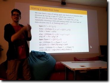
Presented McBride's seminal
paper on zippers (that was sadly never published AFAIK) at
Papers We
Love's Singapore chapter (slides and Haskell implementation
available here).
- Back in October, the self-interpreting in Fω paper started making huge waves in PLT circles. I was only three pages in when I knew I had to present it at Papers We Love. The eventual talk took a couple weeks to prepare for, but it was worth it because it went really well.
Functional programming
- Fixed a long-standing bug in MetaFun, the "Haskell"-to-C++ template metaprogram compiler: patterns in function definitions are now tried for matching in the correct order.
- Wrote a Bison summary parser that a co-worker wanted to use to generate exhaustive test cases for Bison-generated parsers. That project ended up not going anywhere as far as I know.
- If you use every GHC extension and then some, you can write a fairly nifty untyped-to-typed embedding of STLC that is almost as nice as doing it in a proper dependently typed language!
Stack Overflow highlights
Some of the answers I wrote this year on Stack Overflow required me to learn just enough of something new to be able to answer the question:
- Learned just enough about Uniplate to figure out how to do out-of-band code generation.
- Learned just enough about Persistent to figure out how entity keys are represented on SQL database backends.
- Learned just enough about Spock to figure out how to store state between handler invocations (spoiler alert: it's horrible).
- Learned just enough about data-reify to figure out how to observe sharing in a graph
- Learned just enough about Pipes to figure out not just how to generalize runEffect, but also a way to get notified about the end of the input.
- Learned just enough about Accelerate to figure out marshalling of Arrays.
- Learned just enough about Template Haskell to figure out how to create and use custom annotations. OK, so maybe this isn't strictly true, as Template Haskell is something I've known already, but the annotations stuff was definitely new.
- Learned just enough about Euterpea, and the Karplus-Strong algorithm, to figure out how to synthesize a plucked string-like sound out of thin air and white noise.
- Learned just enough about GHCJS to figure out how unboxed Vectors can be efficiently marshalled to Javascript.
- Learned just enough about GHC's RULES facility to figure out how to wrangle it to submission when rewriting overloaded functions.
- Learned just enough about LLVM and GHC's run-time system to figure out how to present handwritten LLVM assembly to GHC as a prim-op.
Then, there were those where it turned out there was a bug to be found by scratching the surface of the question deep enough:
- I've found a bug in Idris's typechecker in the face of typeclass polymorphism
- Even though Tardis and rev-state should be mostly the same code (and they are even written by the same developer!), the latter's MonadFix instance had a one-character, fatal flaw.
Then there were the answers that were just too much fun to write:
- A small romp in integer arithmetic to implement rational addition in Agda
- Reimplementing Parsec in Idris because I was too lazy to look into Lightyear.
- What is the codensity-like representation of MonadPlus? This paper answers the question by wonderfully building up a generalization of DList and Codensity for something which is almost MonadPlus. I ended up writing a summary of the paper.
- Having worked on GHC two years ago to implement pattern synonyms, with the understanding of GHC's type checker internals still fresh in my mind, I was just the right person to explain the GHC code base's usage of the word zonking.
All in all, it seems this has been quite a productive year for me out of the office, even if you exclude the Stack Overflow part. I was actually surprised how long this list was while compiling it for this blog post. Maybe I should write a list like this every year from now...
Initial version of my Commodore PET
2 March 2015 (programming haskell FPGA electronics retro)In my quest to build more and more complicated computers on FPGAs armed with nothing but a crappy hobbist mindset and some hazy ideas of how Kansas Lava is supposed to work, I've reached another milestone: my first real computer.
That is, unlike the Brainfuck CPU that I designed myself, or the CHIP-8, which was originally a virtual machine spec (with all the implementation leeway that implies), this latest subject is a bona fide 8-bit home computer from the seventies: the Commodore PET.

The Commodore PET in a nutshell
The PET is a very simple machine compared to later Commodore models, which is why I thought it would make a good first step on a journey that I hope will one day culminate in implementing a Commodore 64. Its centerpiece is the MOS 6502 CPU (practically the same as the MOS 6510 used in the C=64), and there are only four other components: a text-only video signal generator and three IO interface chips (two PIA's and one VIA) for keyboard, Datasette and extension port communication. Just hooking up one of the PIAs is enough to get a minimal system working with keyboard input.
12 KBytes of PET ROM contain implementation of basic IO routines (the so-called "kernal"), the full-screen text editor, and Microsoft's BASIC interpreter. Then there's a separate character ROM (not addressable from the CPU) used by the video generator.
MOS 6502
The 6502 microprocessor was a staple of the eight-bit home computer era of the late seventies and eighties. By today's standards, it is incredible to imagine what it must have been like to design it manually, drawing the layout with pencils on paper. On the other hand, if it was designed in such a low-tech way, I figured it shouldn't be too difficult to build something compatible using modern tools even by a hobbist like myself. And of course there are already dozens of home-built 6502 implementations out there, to varying degrees of compatibility.
The ultimate reference on the 6502 must be the Visual 6502 Project which I deliberately avoided consulting. I don't really see the educational value in copying the original 6502 design; so instead, I went with a more black-box approach by just looking at the opcode descriptions and interrupt model and working from that.
The first milestone I aimed for was to get enough of the CPU working that I can run the sample programs on 6502asm.com, which defines a tiny microcomputer-like architecture that doesn't have interrupts or any fancy video modes: you just have 32×32 pixels with a fixed 16-color palette mapped to main RAM from $0200, and a zero page-mapped register for keyboard input that you can do polling on. The Kansas Lava implementation is really simple and I plan to reuse it later if I do a similar project with the Z80.
My workflow was that I would use ca65 to assemble test programs, burn them into ROM, and run it in the Kansas Lava simulator for a couple thousand cycles; then render the video RAM into a GTK+ window. I would start with this program that does nothing but moves data around in memory (drawing the Commodore logo pixel by pixel), and basically I implemented the 6502 opcodes as I went along. After two days of work, I finally got it working:
![]()
Seeing this was an incredible feeling. The input was valid 6502 machine code, and my very own CPU managed to run it correctly for the approximately 40,000 cycles that it took to draw this image. There was no stopping at this point: I already had a working VGA frame buffer implementation from the CHIP-8, so next day I synthesized it and run it on real hardware, my venerable Papilio Pro:
![]()
Simulation-based testing
As I added more and more opcodes and started running more and more complicated programs, things very quickly stopped working. My CPU was full of bugs, and figuring out what went wrong by looking at the simulation logs after running it for tens of thousands of cycles was very tedious.
And so, it was at this point that I started adding unit tests. The framework for writing tests exposes a monad where the available effects are making observations on the state of the system (CPU registers and contents of the memory) and executing instructions. This presents an API that allows writing tests in an imperative way:
php = do
    flags <- observe statusFlags
    sp <- observe regSP
    execute0 0x08
    sp' <- observe regSP
    pushed < observe $ mem (stackAddr <$> sp)
    assertEq "Stack pointer is decremented" sp' (pred <$> sp)
    assertEq "Status is correctly pushed" pushed flags
A test like this is turned into a ROM image containing $08 at the address pointed to by the reset vector. The simulation is then run until the CPU enters the Fetch internal state for the second time (the first time is when it fetches the opcode under testing, i.e. the PHP ($08) instruction), and then the observations are evaluated by looking at the simulation output in the same cycles as the Fetch state. Of course, this means you shouldn't be able to write tests like the following:
impossiblyDynamicTest = do
    arg <- observe regX
    execute1 0x00 arg
    a' <- observe regA
    assertEq "A is updated" a' arg
This is ensured by observe returning values wrapped in an Obs type, and execute1 requiring unwrapped arguments:
observe :: Query a -> TestM (Obs a)
execute1 :: Byte -> Byte -> TestM ()
assertEq :: (Eq a, Show a) => String -> Obs a -> Obs a -> TestM ()
To allow assertions over derived values, Obs is an applicative functor (in fact, it is the free applicative functor over the co-Yoneda functor of the primitive observations).
I think this approach has merit as a general framework for hardware simulator-based unit testing and I intend to extend it and maybe even carve it out into a separate library in the future.
A Minimal Viable PET
Once I had a sufficiently working CPU, I started building the other pieces around it. I took the PET emulator from the VICE suite and commented out all the PIA and VIA code, replacing writes with nops and reads with hardcoded values, until I was able to boot it up with the stock ROM to get to the READY. prompt. Of course, since the PIA supplying the interrupt used for timing was removed by that point, I had no flashing cursor or keyboard input. All in all, the system got to a steady state in about 80,000 operations. (Since my implementation is not yet cyle-accurate, I had to switch to counting operations instead of cycles beyond this point. Every operation is at least as fast as on the real chip, so I hope by adding some wait cycles I'll be able to take care of this at some later point.)
After hooking up the same hardcoded values on the same addresses to the CPU, the next step was running the simulator and peeking at the video memory area ($8000..$8FFF on the PET), using the original fonts to render the screen. The initial version showed there might be someone home (sorry for crap quality on the screenshot):

By comparing detailed logs from running the emulator and the simulator, I was able to make observations like "the first 12,345 steps seem to be in agreement", which was a big boost to productivity, getting me, in short order, to this:

After fixing some more bugs in the arithmetic opcodes, I was finally rewarded by this sight:

Adding more components
While working on the CPU, I also started writing the character generator, on top of the VGA signal generator in the kansas-lava-papilio package that I originally made for the CHIP-8. This way, the VGA synchronization signals were abstracted away from me and I just had to take care of pumping out the actual pixels. This turned out to be tricker than I originally thought, since you have to time all read-aheads just right so that everything is at hand just in time for the next pixel. So before it finishes drawing the 8 pixels that make up a single row of a character, the next character index is loaded from RAM, and then the character ROM is consulted for the first row of the font image of the next indexed character. Initial versions were having some ghosting issues, or even more fun, full character transpositions (like showing the character from one line above in the first position of each line).
The Commodore PET diverts the vsync signal from the video generator to one of the PIA chips, which generates a CPU interrupt that can be acknowledged by reading from one of its memory-mapped registers. So the next obvious step was to implement this functionality to get the cursor blinking! This required more than just implementing a PIA, since I didn't even have interrupts in the CPU at that point.
But all that work was totally worth it:
And now, here we are
The current version supports keyboard input from PS/2 keyboards (but not all keys are mapped yet), so for the first time since I started working on this more than a month ago, it can be used to write and run BASIC programs!
What you can't see on the video below is that there's still a bug somewhere that causes the classic 10 PRINT "FOO": 20 GOTO 10 program to terminate with an out of memory error after some time.
Apart from fixing these bugs, the big outstanding feature is to add Datasette support so that programs can be loaded and saved to virtual "casettes". For a first version, I'll just burn some extra ROM onto the FPGA containing the tape images and hook that up to the PIA controlling the casette player; but I guess the proper way to do this would be to use something like an SD card reader to get proper persistent, read-writable storage. Or maybe, alternatively, have some kind of serial-over-USB communication with a computer acting as the Datasette unit.
My first computer
29 March 2014 (programming haskell FPGA electronics retro)tl;dr: I've built a computer on a Xilinx FPGA using Kansas Lava, based on a virtual machine design from the mid seventies.
I would be lying if I said I always wanted to build my own computer. For a very long time, hardware didn't tickle my curiosity at all; and even today, I prefer staying away from dangling wires and soldering irons. I like my computing platforms to Just Work, and hardware problems are just a huge hassle. But then in 2010 some coworkers of mine started getting into electronics and I learned from them just enough to start hooking some ICs up on a breadbord, and it seemed like a very fun diversion from all the high-level, abstract, softwarey stuff. In some sense, it filled the same void in me that assembly programing would probably have had. But even back in the days on the Commodore 64, I was looking for more BASIC extensions instead of going downwards to assembly / machine code.
One thing led to another and I was creating a Brainfuck CPU on a Papilio FPGA. It was a very satisfying experience, plus, I got to learn about a completely new world (that of digital hardware design and hardware description languages). So ever since then, I had a voice in the back of my head saying I should go all in, and implement a proper full computer, with I/O and all. But jumping straight into replicating a real computer seemed like trying to run before I can walk.
I can't remember now how I bumped into the CHIP-8 platform, but when I read about it in detail, I realized this is something I, a self-taught HDL guy, could realistically implement. To recap, it's a virtual machine spec from the mid seventies indended to be implemented on home computers of the time. It is super low performance, meaning I could implement everything the most naïve way possible and still get something workable out of it: graphics is 64×32 black & white, RAM is short of 4KBytes, CPU speed is not really part of the spec, and the only timers provided run at 60 Hz.
I can do this!
Setting the scene
The FPGA board that I targeted is a Papilio One 500K, which has 500K... somethings called "system gates", and about 40KByte of SRAM. The Arcade MegaWing provides a D-sub 15 VGA connector and two PS/2 ports, among some other stuff that I am not using for this project.
The home computer targeted by the original CHIP-8 spec only had a four-by-four keypad, so I am not 100% happy about using a PS/2 keyboard for the input. Maybe a later version could use a bespoke keypad connected to the unused pins of the LogicStart MegaWing. However, by using a PS/2 keyboard, I could not worry about the hardware side of things and just implement a decoder for the PS/2 protocol.
In terms of software, there are several games available for the CHIP-8. Maybe even donzens! But just for fun, after finishing the machine itself, I ended up writing my own game as well: a crappy port of the currently trending 2048 game.
Understanding the CHIP-8
I would say the CPU itself is a RISC architecture, in that it has 16 registers and not a whole lot of operations. But I'm not sure it would be called RISC back in its day.
The aforementioned 64×32 one-bit graphics is manipulated via a sprite interface: there's a special CPU opcode for xor-blitting an 8-pixel-wide, variable-height sprite onto any part of the screen. I went with the obvious way of implementing it as a 2048-bit frame buffer.
To validate my understanding, I first created a software emulator in Haskell. That unearthed a ton of edge cases and situations where I was not reading the spec with enough attention. Once I had the emulator working well enough to play the sample games I found, I enumerated the modules I'll need to implement.

A TODO list
Since I've already done the Brainfuck CPU, I didn't foresee too much difficulty in implementing the CPU proper (oh boy was I wrong). However, the world of peripherals was a new one to me.
I've never looked into VGA signal timings in detail before, and for some reason I just assumed that it's going to be just as complicated as PAL, about which I knew just enough to know that you have to generate all kinds of elaborate sync patterns. So actually reading the VGA spec was a relief, and I quickly came up with a scheme where my CHIP-8 computer would be running at 50 MHz, so that it can easily implement the 25 MHz pixel clock needed for 640×480@60 Hz. I went with this mode because it has several advantages:
- It refreshes the screen at 60 Hz, so I can synchronize the CHIP-8 timers to it
- It has square pixel aspect ratio
- It is a "default" mode, so I can be confident that if I generate the correct signal, modern LCDs will be able to display it. In fact, for testing, I later got a 7" CCTV LCD with a VGA input on the cheap, so that I didn't have to make room for the 21" TFT I had lying around. The CCTV monitor supports three VGA video modes, and 640×480@60 Hz is one of them.
- By dividing both the horizontal and vertical resolution by 8, I can get 80×60 which doesn't leave too much unused border around 64×32. I could use all horizontal screen real estate if I divided by 10 instead, to get 64×48, but I have no idea how I could divide my horizontal/vertical position counter by 10; whereas dividing by 8 is a simple matter of shifting to the right by 3 bits.
The Papilio One itself has a clock of 32 MHz, and I first hoped that 32 Mhz and 25 Mhz is close enough that I can just generate a signal using the 32 MHz as the pixel clock. Turns out that's not quite how signal timings work.
Luckily, I've found out that the Papilio One also has something called a DCM which can divide and multiply the clock signal. I was able to go to 25 or 50 MHz easily with it. It's a bit of a black box component: I had to run a wizard in the Xilinx IDE to get a small binary file describing my DCM parameters, and then I integrated it into my build process by running another Xilinx program on it which spits out some magic bitstream.
The PS/2 protocol is a simple serial protocol with a slow (~10 KHz) clock and one parity bit per 8 data bits. Decoding it into a stream of bytes was a straightforward thing once I hunted down an actual PS/2 keyboard, since it turned out those USB to PS/2 dongles don't really work with regular USB keyboards; rather, the keyboard have to be made ready to "speak" PS/2 over the dongle. So I ended up getting a proper PS/2 keyboard from Mustafa Centre (thanks to Viki's sister Dori for picking it up for me); god only knows why they still had one on stock.
Tooling
The Xilinx tool suite seems to be aimed at being used from the IDE. This has several drawbacks: version controlling is complicated because generated artifacts litter the source tree; the editor itself in the IDE is of course crap compared to Emacs; and most importantly, I didn't intend to manually write either VHDL or Verilog. As I've mentioned before in my post about the Brainfuck CPU, I've found both of these hardware description languages to be lacking in the same way mainstream imperative programming languages are: the tools you, the developer, is given to introduce your own abstractions are very poor. So I planned to use Kansas Lava, an HDL embedded in Haskell.
Now, the first thing to note about Kansas Lava is, as nice at is, the software package itself is bit-rotten. The latest version available on Hackage cannot even be compiled with GHC 7.6. While the change to fix that is trivial, after that, you can easily bump into bugs in the Lava compiler itself. But more on that later. Later versions available from GitHub are not even self-consisent between the various dependencies. I've put my patched-up version of Kansas Lava and some of the packages it dependens on on GitHub and I'm trying to get Andy Gill to allow me to upload the bundle as a 0.2.4.1 update to Hackage. Don says I should maybe say fuck it and create my own Singapore Lava fork, just to stay with the Lava tradition of a twisty little maze of incompatible forks, all alike.
However, when it all works, it is amazing. I was able to extend the library of Papilio-specific Lava code that I created for the Brainfuck project with reusable modules for the VGA signal generator and the PS/2 decoder in such a way that they should be very easy to be re-used for any other future projects. And it's all type-safe, so for example, the Papilio Arcade MegaWing VGA port is statically enforced to be 4+4+4 bits whereas the LogicStart MegaWing is 3+3+2.
But there was one bug that left a bitter aftertaste in my mouth. Once I had both the CPU and the VGA parts working and I started running some test programs on the thing, I noticed that the framebuffer blitting is exhibiting "or" behaviour instead of "xor". Running the same code in the Lava simulator and dumping the contents of the framebuffer, it showed the correct, "xor" behaviour. After weeks of frustration and a complete rework of the communication system between the CPU, the VGA signal generator and the frame buffer to add memory read bussing, I finally took a look at the Lava compiler's source code to find that it simulates the xor2 primitive as xor but compiles it to or. How do you not notice this bug? Has the Kansas Lava suite been used by anyone for everything at all in the history of ever???
End result
The final result, after much trial and error, looking at the Lava simulator's output, and pouring over the code, is available here. I'm reasonably happy about the code base, except for the implementation of the CPU itself, which feels a bit spaghetti to me. Especially around the parts where it's waiting for results to come back from main RAM or the video framebuffer.
Below are some photographs and videos of it running two games: the memory puzzle game Hidden and the 2048 clone mentioned above. Unfortunately, the Tetris game from the screenshot above seems to have a bug in its input handling, in that it samples the keyboard at an unthrottled frequency; thus, even the shortest keypress sends the falling piece to the edge of the wall. I'll eventually need to disassemble the game and fix this.
The VGA signal generator is not as neat as it could be, because it doesn't do pre-fetching. This means by the time the current CHIP-8 pixel's value is read from the framebuffer, it is already too late, the first of the 8 real pixels for the given virtual CHIP-8 pixel should already have been drawn. This results in some ghosting. But since I know what's causing it, I will hopefully be able to fix this in some next version. But right now I'm too happy to have the whole thing just working.


A Brainfuck CPU in FPGA
19 January 2013 (programming haskell brainfuck FPGA electronics ISC) (3 comments)About two and a half years ago, a wave of interest in electronics swept across the Budapest office of Intentional. We desperately wanted to create something tangible from first principles. The idea we settled on was to design and eventually build a CPU that uses Brainfuck as its machine language.
Looking back, it really was a case of people with insufficient knowledge trying to use inappropriate tools. But damn if we didn't have fun during the process! After filling a couple of notebooks with sketches, we ended up with an initial design in Logisim. It had horrible timing problems, of course, since too much of it was asynchronous. Before ironing out all the wrinkles, though, I remember Maya pointing at one of the lines tangled up on the screen, and saying "You guys realise this single line will be 16 wires if we actually want to solder this together, right?" So basically we gave up on building the thing. Later on, Maya and Encsé went on to enroll to a bachelor's program in EE as a hobby; and I decided to stick to discrete logic, ordered a bunch of 7400 TTL's and some LEDs and seven-segment displays and started wiring together much simpler circuits on breadboards. I never got to soldering, not to mention getting access to anything that could produce PCB's, Then as I moved to Singapore, I left all my electronics stuff at home, and put the whole electronics thing on the backburner indefinitely.
Then, a couple months ago I discovered the Papilio FPGA platform, which has this collection of nice IO daughterboards (called "wings") that snap right into it, no soldering or even wiring required. I ordered one with the LogicStart IO board which features, among other, more advanced stuff, eight toggle switches and four seven-segment displays. Perfect for my baby steps into the world of FPGA's!
So what else could my Hello World project have had been, than the Brainfuck CPU.
Basic design
We can use the Harvard architecture: since the Brainfuck language has no reflection capabilities, the program can be stored in ROM with no programmable access. Memory is implemented as a RAM of 32K 8-bit bytes. The CPU also has several internal registers:
- Internal state: As we will see, it takes several clock cycles for the CPU to execute a given Brainfuck opcode. Rather unfortunately, I ended up with 9 states, so I need 4 bits to store it.
- Program counter (PC): directly connected to the address pin of the ROM.
- Opcode register: loaded from the data pin of the ROM in the Fetch state.
- Memory pointer (idx): a 15-bit register that is directly connected to the address pin of the RAM.
- Data out register: for simplicity's sake, new values for RAM[idx], and the write enable leg of the RAM, are buffered
- Depth counter (DC): Used in the implementation of the [ and ] opcodes (see below)
Output is implemented by an 9-bit signal: 8 bits of data and an enable bit. When a . opcode is encountered, the CPU sets these 9 bits, and enters a special state until it receives an acknowledgment signal. Input is implemented similarily. On the actual board, the output signals are connected to the seven-segment display, the input signals are fed from the eight toggle switches, and the directional "mini-joystick" is used to acknowledge input/output.
Implementing [ and ]
Compared to a normal machine language, it's really just [ and ] that requires special handling. Everything else is just straightforward manipulation of either idx or RAM[idx] via incrementing/decrementing; or pushing data between RAM[idx] and the IO port. [ and ] are tricky because we need to search for their matching pairs, and pre-processing the Brainfuck program to attach pair addresses would be against the spirit of this (self-imposed) challange.
One solution would be to maintain a stack in a separate RAM, and push PC into it whenever a [ is encountered. In that case, ] is a simple matter of popping PC if RAM[idx] does not equal 0. However, here we've basically changed [/] from a while loop to a do while loop. So if RAM[idx] is 0 when we first enter the [, we have to scan the program forward to find its matching ].
For simplicity's sake, I decided not to worry about performance and skip the stack part, and just implement scanning in both directions. Scanning is where the DC register is used (explained here for [, but ] is similar): if the opcode is [ and RAM[idx] is 0, DC is set to 1, and the CPU enters a special skip-forward state from the next opcode. In this state, only [ and ] opcodes have any effect: they increment and decrement, respectively, the DC register. When DC gets to 0, we know we've found the matching ], and so we can go back to the regular fetch-execute cycle.
Lava → VHDL → Xilinx
I originally planned to implement the whole thing in VHDL, and compile that using the Xilinx synthesizer tools (since the Papilio One board uses a Xilinx FPGA chip). However, I've found VHDL to be quite a horrible language from a software programmer's point of view. The whole point, for me, of going from physical chips to FPGA's was to enable using abstractions to manage complexity; so why settle for a poor language like VHDL? Fortunately, there's a whole family of Haskell-embedded DSLs for hardware description called Lava. Of these, Kansas Lava seemed the only one actively maintained, and it already had support for a Xilinx dev board; so adding support for the Papilio was straightforward (see my kansas-lava-papilio package).
The complete code for my Brainfuck CPU (including IO via the LogicStart daughterboard) is available on GitHub. There are quite some rough edges left to file off; I'd say the most pressing is adding the ability to synthesize the program ROM separately from the CPU definition.
Videos
This first video shows a simple countdown (actually, count-up) program: ,[>+.<-]. I had to record these slightly out-of-focus, otherwise the seven-segment LEDs were hard to read.
Next up is "Hello world!":
And the final one shows Maya's solution to the 9-digit problem. This one really shows how slow this naïve, stackless implementation is.